Top 7 PCB Design Mistakes That Increase Manufacturing Costs
1️ Designing at the Absolute Minimum Trace/Space Limits
The Mistake
Designing trace/space (e.g., 3/3 mil or below) across the entire board when it is not electrically necessary.
Engineers often:
Default to tight rules from HDI designs
Copy constraints from another project
Assume “smaller is better”
Why It Increases Cost
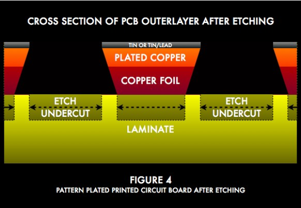
- Requires higher-end imaging capability
- Slower etching process
- Increased scrap rate
- Avoid common fabrication mistakes
- Tighter registration tolerances
- More AOI time
- Often forces premium fabrication pricing
- Yield drops significantly as trace width shrinks.
- A 4/4 mil board may cost dramatically less than a 3/3 mil board — even though the difference seems minor.
- A 4/4 mil board may cost dramatically less than a 3/3 mil board — even though the difference seems minor.
How to Avoid It
- Use fine traces only where electrically required
- Keep power areas and non-critical routing at relaxed rules (5/5 or 6/6 if possible)
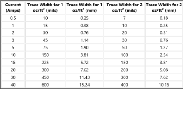
- Match trace width to current requirement, not aesthetic preference
- Match trace width to current requirement, not aesthetic preference
- Discuss fabricator’s standard capability before locking rules
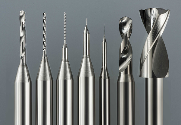
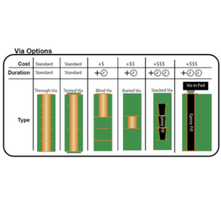
2️ Using Excessively Small or High Aspect Ratio Vias Everywhere
The Mistake
- Specifying very small drills (e.g., 6 mil finished or below) or high aspect ratio vias across the entire design.
- Often caused by:
- Over-optimizing density
- Using HDI practices on standard boards
Why It Increases Cost
- Smaller drill bits wear faster
- Slower drilling cycle time
- Higher breakage rate
- More difficult plating uniformity
- Reduced reliability margin
- High aspect ratio vias (depth ÷ drill diameter) increase risk of:
- Voids
- Reliability failures in thermal cycling
- Many shops consider >10:1 aspect ratio “premium build.”
How to Avoid It
- Use standard drill sizes when possible
- Keep aspect ratio under 8:1 for best cost/yield
- Avoid shrinking vias unless routing density demands it
- Consider design redistribution instead of via reduction
- Ask for fabricator drill capability table early
- Practical Tip:If your board thickness is 0.062", an 8 mil finished hole is far safer than 6 mil — and often much cheaper.
Why These Two Mistakes Matter
- Both issues:
- Reduce manufacturing yield
- Increase scrap
- Increase inspection time
- Push your board into a higher cost capability tier
- And most importantly — they are usually unnecessary.
Quick Cost-Reduction Checklist
- Are we using the smallest trace width everywhere?
- Are all vias smaller than necessary?
- Is aspect ratio reasonable?
- Did we confirm standard shop capability first?
- These two design habits alone can swing PCB pricing by 15–40% depending on layer count and complexity.
- If you’d like, I can also provide:
- 5 more common cost drivers
- A DFM audit checklist
- Or a “PCB cost reduction playbook” written for engineers
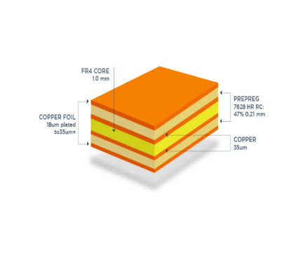
3️ Unbalanced Copper Distribution
The Issue
- Large copper planes on one layer and sparse routing on the opposing layer.
Why It Increases Cost
- Causes bow and twist during lamination
- Creates plating thickness variation
- Increases scrap rate
- May require copper thieving or process adjustments
How to Control It
- Balance copper density layer-to-layer
- Use copper thieving where needed
- Keep stackup symmetrical
- Copper balance directly affects yield.
Why These Two Mistakes Matter
- Both issues:
- Reduce manufacturing yield
- Increase scrap
- Increase inspection time
- Push your board into a higher cost capability tier
- And most importantly — they are usually unnecessary.
4️ Over-Specifying Controlled Impedance
The Issue
- Calling out tight impedance tolerances (±5% or tighter) on traces that don’t require it.
Why It Increases Cost
- Requires modeling and engineering review
- May require dielectric adjustments
- Often forces tighter process control
- Adds TDR testing
How to Avoid It
- Apply impedance control only to high-speed nets
- Use ±10% tolerance unless tighter is truly required
- Confirm dielectric thickness availability
- Not every signal needs impedance control.
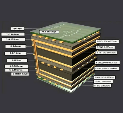
5️ Excessive Layer Count
The Issue
- Adding layers instead of optimizing routing.
Why It Increases Cost
- Each layer adds material and lamination cost
- Longer lamination cycles
- Higher risk of registration errors
- More AOI inspection
- Going from 6 layers to 8 layers is not a small jump — it can increase cost 20–35%.
How to Control It
- Optimize ground/power plane strategy
- Re-evaluate via structure
- Confirm routing congestion is truly layer-limited
- Layer count is one of the biggest price multipliers.
6️ Via-in-Pad (Filled and Capped)
The Issue
- Placing vias directly in SMT pads and requiring fill + planarization.
Why It Increases Cost
- Additional drilling cycle
- Via fill material
- Planarization process
- Extra inspection
- Often requires sequential lamination
- This can push a board into HDI pricing.
How to Control It
- Use dog-bone fanout where possible
- Reserve via-in-pad for dense BGA only
- Clarify conductive vs non-conductive fill
- Use only where routing density demands it.
7️ Special or Exotic Materials
The Issue
Examples:
- RF materials
- Polyimide
- Low-loss laminates
Why It Increases Cost
- Higher raw material price
- Longer procurement time
- Special lamination parameters
- Increased scrap risk
- Material cost alone can double board price.
How to Control It
- Confirm electrical requirements justify it
- Evaluate high-Tg FR-4 first
- Ask fabricator about stocked materials
- Material choice often drives both cost and lead time.
| Cost Driver | Impact Level |
|---|---|
| Copper imbalance | Medium–High |
| Overuse of impedance control | Medium |
| Extra layers | High |
| Via-in-pad | High |
| Exotic materials | Very High |
Engineering Reality
- Most PCB cost increases come from:
- Designing at process limits
- Over-specifying requirements
- Copying constraints from previous designs
- The most cost-efficient boards:
- Engage the fabricator before layout is frozen