Ceramic PCB Design
Ceramic PCB Design GuideCeramic Printed Circuit Boards (PCBs) replace the traditional FR-4 fiberglass-epoxy substrate with high-performance ceramic materials. They excel in high-temperature, high-power, high-frequency, and high-reliability applications where standard PCBs fail.Why Use Ceramic PCBs?
- Superior thermal conductivity — 20–100x better than FR-4.
- High operating temperatures — Up to 350–800°C.
- Excellent electrical insulation and low dielectric loss.
- Low CTE (Coefficient of Thermal Expansion) — Matches silicon chips better, reducing stress.
- Dimensional stability and vibration resistance.
- Near-zero moisture absorption.
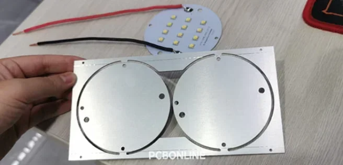
- Common Applications: High-power LEDs, power electronics, RF/microwave circuits, aerospace, automotive (EV power modules), medical devices, and downhole tools.
Why Use Ceramic PCBs?
- Superior thermal conductivity — 20–100x better than FR-4.
- High operating temperatures — Up to 350–800°C.
- Excellent electrical insulation and low dielectric loss.
- Low CTE (Coefficient of Thermal Expansion) — Matches silicon chips better, reducing stress.
- Dimensional stability and vibration resistance.
- Near-zero moisture absorption.
- Common Applications: High-power LEDs, power electronics, RF/microwave circuits, aerospace, automotive (EV power modules), medical devices, and downhole tools.
- Thermal Conductivity Comparison (Relative to FR-4 ≈ 0.3 W/m·K):
- Alumina (Al₂O₃): ~20x
- Aluminum Nitride (AlN): ~100–170x
- FR-4: 1x
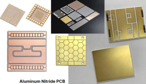
- Common Ceramic Substrate Materials
Material
- Thermal Conductivity (W/m·K)
- CTE (ppm/°C)
- Dielectric Constant (Dk)
- Key Advantages
- Drawbacks
- Typical Use Cases
Key Design Considerations for Ceramic PCBs
1. Board Size & Thickness Limits
- Ceramics are brittle → Maximum panel size often ~140 × 190 mm (varies by manufacturer).
- Common substrate thicknesses: 0.38 mm, 0.5 mm, 0.635 mm, 0.8 mm, 1.0 mm, 1.5 mm, up to 3.0 mm.
- Thinner boards = better thermal performance but more fragile.
2. Layer Count
- Prefer single-layer or double-sided designs.
- Multilayer (up to 4 layers) is possible but risk of cracking during lamination increases significantly. Use only when necessary.
3. Copper Thickness & Trace Design
- Typical copper: 1 oz (35 µm) to heavy copper (up to 10 oz or direct bonded copper – DBC).
- Wider traces and larger pads recommended due to manufacturing processes.
- Use thermal reliefs carefully — ceramics already spread heat extremely well.
4. Thermal Management
- Place high-power components (MOSFETs, LEDs, ICs) to maximize contact with the ceramic substrate.
- Use thermal vias liberally (larger diameters preferred).
- Consider Direct Bonded Copper (DBC) or Direct Plated Copper (DPC) for best thermal path.
5. High-Frequency / RF Design
- Stable Dk across temperature.
- Lower loss tangent than FR-4 at high frequencies.
- Controlled impedance traces are easier to maintain due to material stability.
6. Component Placement & Mechanical
- Avoid large/heavy components near board edges.
- Account for brittleness — add mounting holes with proper clearance.
- Use CTE-matched components.
7. Vias & Holes
- Laser drilling common for small vias.
- Plated through-holes (PTH) possible but more expensive.
- Blind/buried vias limited in multilayer ceramics.
8. Surface Finish
- ENIG (Electroless Nickel Immersion Gold) is most common.
- Others: OSP, Immersion Silver, or thick gold for wire bonding.
Manufacturing Technologies for Ceramic PCBs
- DBC (Direct Bonded Copper) — High thermal, thick copper.
- DPC (Direct Plated Copper) — Fine lines, good for RF.
- Thick Film — Screen printing + firing.
- Thin Film — For very high precision.
- LTCC/HTCC — For multilayer ceramic modules.
- Design Rules of Thumb (Typical Values)
- Minimum Trace Width/Space: 0.15–0.25 mm (depends on process).
- Minimum Hole Size: 0.2–0.3 mm.
- Annular Ring: ≥0.1 mm.
- Solder Mask: Often omitted or use high-temp white/black mask.
- Clearance to Edge: ≥0.5 mm.
- Always run DFM with your ceramic PCB manufacturer early.
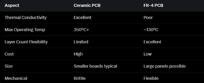
Ceramic vs FR-4 Design Summary
Best Practices & Tips
- Collaborate with your manufacturer from the design stage (many offer free DFM).
- Use simulation tools (thermal + electrical) — ceramics change design assumptions.
- For assembly: Higher reflow temperatures (up to 400°C+) are possible.
- Add fiducials and tooling holes carefully.
- Ceramic PCBs enable designs that would be impossible or unreliable with FR-4. While they cost more and require careful handling, they provide unmatched performance in demanding environments.If you're working on a specific project (e.g., high-power LED, RF amplifier, or power module), share more details and I can provide tailored layout recommendations!