Top 7 PCB Design Mistakes That Increase Manufacturing Costs
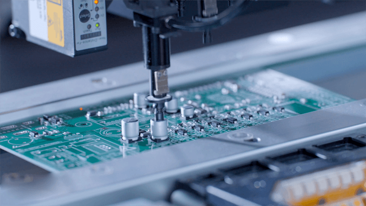
PCB Manufacturing Process
Customer Training Manual
(Engineering-Level Overview for Buyers & Program Managers)
1. Purpose of This Manual
- This document is intended to help customers:
- Understand how printed circuit boards are manufactured
- Design with manufacturability in mind (DFM)
- Avoid common fabrication mistakes
- Improve yield, cost, and lead time
- Communicate clearly with PCB fabricatorsyield, cost, and lead time
- This guide assumes familiarity with Gerber files, stackups, and assembly processes.

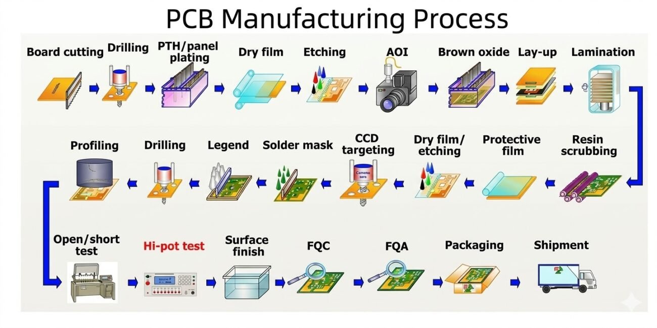
2. PCB Manufacturing Overview
High-Level Fabrication Flow:
- Data review (CAM/DFM)
- Inner layer imaging & etching
- Layer lamination
- Drilling
- Copper plating
- Outer layer imaging & etching
- Soldermask
- Routing/depanelization
- Electrical test & inspection
3. Data Package Requirements
Required Files:
- Gerber (RS-274X preferred)
- Drill file (Excellon)
- Fabrication drawing
- Netlist (recommended)
- Impedance requirements (if applicable)
Optional but Strongly Recommended:
- Readme notes
- IPC class requirement (Class 2 or 3)
- Controlled impedance tolerance (±5%, ±10%)
Common Customer Mistakes:
- Missing drill tool sizes
- No finished copper weight specification
- Undefined surface finish
- Impedance callouts without dielectric thickness
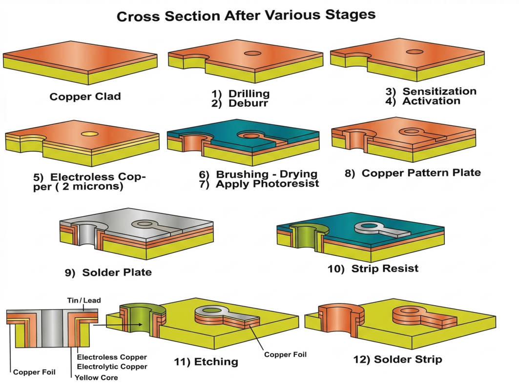
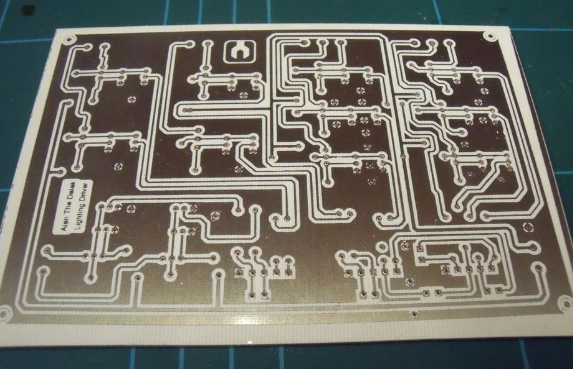
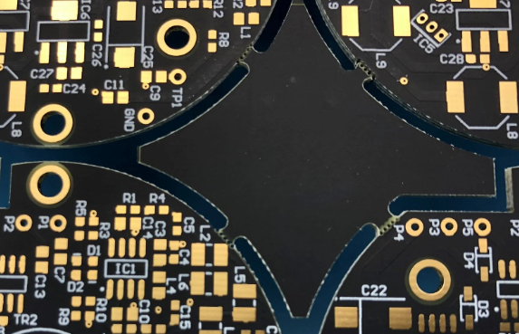
4. Inner Layer Fabrication
- Dry film photoresist applied
- UV imaging defines traces
- Copper etched
- Automated Optical Inspection (AOI)
Customer Impact:
- Fine line designs increase risk
- Tight trace/space raises cost
- Copper balancing affects warpage
Design Guidance:
- Avoid copper thieving imbalances
- Maintain minimum annular ring
- Keep trace width consistent for impedance
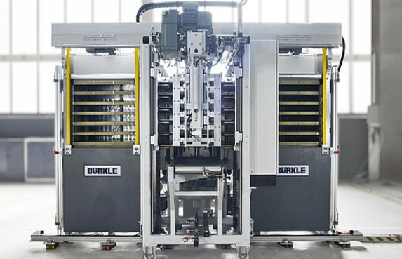
5. Lamination (Multilayer Boards)
What Happens:
- Inner layers stacked with prepreg
- Heat and pressure cure the epoxy
- Final rigid multilayer panel created
Customer Impact:
- Stack-up accuracy affects impedance
- Resin flow impacts via reliability
- Excess copper density may cause bow/twist
Design Guidance:
- Symmetrical stackups reduce warpage
- Balance copper on each layer
- Specify dielectric thickness clearly
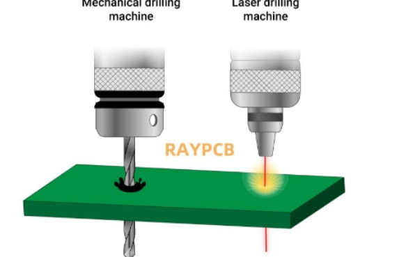
6. Drilling & Via Formation
Via Types:
- Through-hole
- Blind via
- Buried via
- Laser microvia (HDI)
Critical Engineering Limits:
- Aspect ratio (typically ≤10:1 standard)
- Minimum drill size
- Via-to-pad clearance
Customer Impact:
- Small vias increase cost
- High aspect ratio reduces yield
- Stacked microvias increase risk
7. Copper Plating & Pattern Formation
Process:
- Electroless copper deposition
- Electrolytic copper plating
- Pattern plating
- Etching unwanted copper
Customer Impact:
- Trace width reduction during etch
- Via wall thickness affects reliability
- Uneven copper distribution impacts flatness
Best Practices:
- Account for etch compensation
- Avoid extreme copper density shifts
- Specify minimum finished hole copper thickness
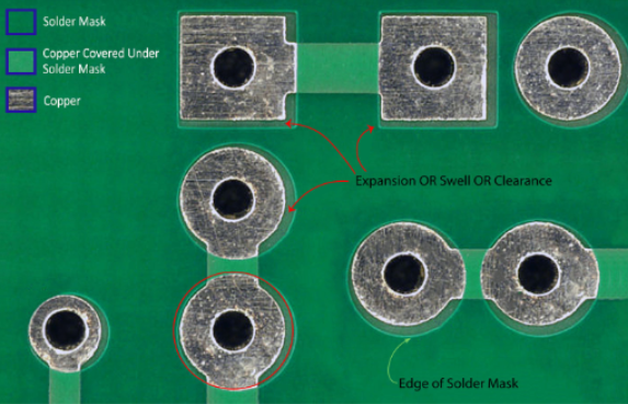
8. Soldermask Application
Purpose:
- Insulates copper
- Prevents solder bridging
- Protects traces
Customer Design Risks:
- Mask slivers between pads
- Inadequate soldermask dams
- Via tenting misinterpretation
Recommendations:
- Maintain ≥4 mil mask dam if possible
- Clarify via tenting intent
- Avoid extremely small mask openings
9. Surface Finish Selection
Common Finishes:
| Finish | Advantages | Considerations |
|---|---|---|
| HASL | Low cost | Uneven surface |
| ENIG | Flat, reliable | Higher cost |
| OSP | Low cost, flat | Shorter shelf life |
Customer Decision Drivers:
- Trace width reduction during etch
- High-reliability → ENIG or Immersion Silver
- Cost-sensitive builds → HASL

10. Routing & Depanelization
Purpose:
- V-score
- Tab route (mouse bites)
- Full route
Customer Considerations:
- Component overhang near edges
- Breakaway stress
- Panel rigidity for SMT
11. Electrical Test (E-Test)
Methods:
- Flying probe (prototype)
- Fixture-based bed-of-nails (volume)
Tests:
- Opens
- Shorts
- Netlist verification
- Always request electrical test unless explicitly waived.
13. Common Customer Mistakes That Increase Cost
- Over-specifying Class 3 unnecessarily
- Calling out unrealistic impedance tolerances
- Using smallest possible vias everywhere
- Excessive layer count
- No copper balancing
- Missing fabrication notes
14. Lead Time Drivers
- Lead time increases with:
- HDI stackups
- Sequential lamination
- Via-in-pad filled and capped
- Tight impedance tolerance (±5%)
- Tight impedance tolerance (±5%)
15. DFM Best Practices Checklist
- Before releasing fabrication:
- Stackup defined clearly
- Copper weights specified
- Surface finish defined
- Impedance callouts documented
- Drill chart included
- Controlled impedance modeling reviewed
- IPC class defined
- Panelization discussed
16. Final Thoughts for Customers
- PCB fabrication is a chemical, mechanical, and thermal process.
- Small design decisions significantly impact yield and reliability.
- The most successful programs:
- Engage fabricator early
- Balance performance and cost
- Avoid designing at absolute process limits