LEAD TIME DESIGN FOR ENGINEERS
primarily driven by design decisions made before fabrication release. Below are the highest-impact engineering controls.
1️ Design Inside Standard Capability Windows
Why It Affects Lead Time
- When your board fits inside standard production capability:
- It skips special engineering review
- It avoids premium process queues
- It moves directly into fabrication flow
High-Risk Design Choices
- 3/3 mil trace/space everywhere
- ≤6 mil finished vias
- 10:1 aspect ratio
- Very tight annular rings
Engineering Control
- Stay at 4/4 mil or larger when possible
- Keep finished vias ≥8 mil for 0.062" boards
- Confirm drill and plating limits early
- Standard builds move faster because they are repeatable.
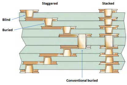
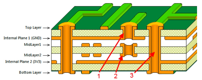
2️ Avoid HDI Unless Density Demands It
Why It Affects Lead Time
- HDI requires:
- Laser drilling
- Sequential lamination
- Extra inspection cycles
- Each lamination cycle can add 1–2 days.
Engineering Control
- Use dog-bone fanout before choosing microvias
- Avoid stacked microvias unless unavoidable
- Prototype with simpler via structures
- HDI boards automatically enter slower production lanes.
3️ Use Stock FR-4 and Common Dielectric Builds
Why It Affects Lead Time
- Non-stock materials require:
- Procurement
- Batch ordering
- Possibly import logistics
High-Delay Materials
- Specialty RF laminates
- Rare dielectric thicknesses
- Heavy copper cores
- Very high Tg not commonly stocked
Engineering Control
- Ask what cores/prepreg are stocked
- Choose common dielectric thicknesses
- Stay with standard 1 oz outer copper
- Material availability can add days before fabrication even begins.
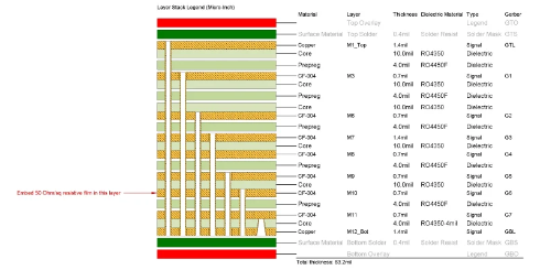
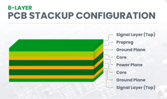
4️ Keep Layer Count Realistic
Why It Affects Lead Time
- Each additional layer:
- Adds imaging cycles
- Adds AOI cycles
- Extends lamination time
- Going from 6 layers to 10 layers can significantly change production flow priority.
Engineering Control
- Optimize plane strategy before adding layers
- Reassess routing congestion
- Balance performance vs. schedule
- Layer count is one of the strongest schedule multipliers.
5️ Simplify Via Structures
Why It Affects Lead Time
- Complex vias require:
- Extra drilling programs
- Filling and planarization
- Additional inspection
- Via-in-pad can add multiple process steps.
Engineering Control
- Use through-hole vias for most routing
- Avoid filled vias unless assembly requires it
- Keep aspect ratio under 8:1 when possible
- Simple vias = faster drilling + plating + inspection.
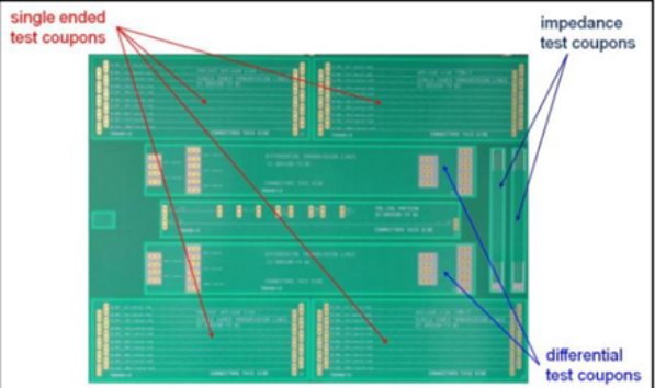
6️ Avoid Over-Tight Impedance Tolerances
Why It Affects Lead Time
- Tight impedance (±5% or tighter) requires:
- Stackup modeling review
- Test coupon creation
- TDR validation
Engineering Control
- Use ±10% unless physics requires tighter
- Apply impedance only to critical nets
- Confirm dielectric thickness availability
- Unnecessary impedance requirements slow CAM release.
7️ Choose Fast-Turn Surface Finishes
Why It Affects Lead Time
Finishes vary in process time:
- Faster
- HASL
- OSP
- Slower
- ENIG (nickel deposition + inspection)
- Immersion Silver
Engineering Control
- Use HASL when flatness is not critical
- Reserve ENIG for fine-pitch or reliability needs
- Finish choice can affect final process queue.
8️ Release Clean, Complete Fabrication Documentation
Why It Affects Lead Time
- The most common delay is documentation clarification.
- Typical Stops:
- Missing surface finish callout
- Undefined stackup
- Conflicting drill sizes
- No IPC class
Engineering Control
- Before release confirm:
- Stackup defined clearly
- Surface finish specified
- IPC class stated
- Drill chart included
- Controlled impedance notes clear
- Clean documentation prevents CAM hold.
Lead Time Risk Ranking
| Design Feature | Lead Time Impact |
|---|---|
| Sequential lamination | Very High |
| Exotic material | Very High |
| 10+ layers | High |
| Via-in-pad | Moderate–High |
| Tight impedance | Moderate |
| Standard 4–6L FR-4 | Low |
Practical Engineer’s Summary
- Fastest-turn boards typically are:
- 4–6 layers
- Standard FR-4
- 0.062" thickness
- 1 oz copper
- No sequential lamination
- Clean documentation
Slow boards are almost always the result of complex structures, rare materials, or over-specification.
Lead time reduction is controlled at the schematic and layout stage — not in the factory.