PCB Design Guide
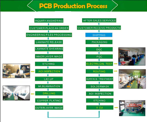
1. Design and Output (Pre-Production Engineering)
Why It Affects Lead Time
- Engineers create the schematic and PCB layout using software like Altium Designer, KiCad, or Eagle.
- They generate manufacturing files: Gerber files (for layers, solder mask, silkscreen), drill files (NC Drill), netlists, and BOM if needed.
- The manufacturer performs a Design for Manufacturability (DFM) check to catch issues like trace widths, clearances, or via sizes.
- It moves directly into fabrication flow
2. Film Generation / Imaging Preparation
- A plotter creates photo films (or uses direct laser imaging in modern processes) from the Gerber files.
- These films act as masks: black areas block UV light, clear areas allow it (patterns reverse for outer vs. inner layers).
3. Inner Layer Printing (for Multilayer PCBs)
- Start with copper-clad laminate (core: fiberglass + epoxy with copper foil on both sides).
- Apply photoresist (light-sensitive film) to the copper.
- Align the photo film and expose to UV light: light hardens the photoresist where copper traces should remain.
- Develop: wash away unhardened photoresist with alkaline solution, exposing unwanted copper.
4. Etching Inner Layers
- Chemical etching (e.g., using alkaline or acidic solutions) removes exposed copper.
- Strip remaining photoresist, leaving only the desired copper traces on inner layers.
5. Layer Alignment, Optical Inspection (AOI), and Oxide Treatment
- Inspect inner layers automatically (AOI) against the original design for defects.
- Apply oxide or black oxide treatment to inner layers for better bonding in lamination.
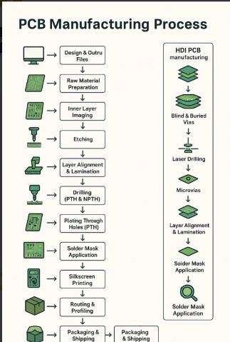
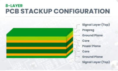
6. Lamination (Layer Bonding)
- Stack inner layers with prepreg (pre-impregnated fiberglass sheets) and outer copper foils.
- Use heat and high pressure in a hydraulic press to bond everything into a solid multilayer panel.
7. Drilling
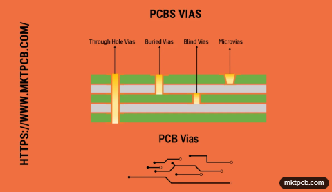
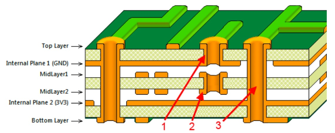
- Drill holes for through-hole components, vias (connections between layers), and mounting.
- Use CNC machines with precise drill bits. X-ray may locate inner features for accuracy.
- Distinguishes plated through-holes (PTH) from non-plated.
Engineering Control
- Ask what cores/prepreg are stocked
- Choose common dielectric thicknesses
- Stay with standard 1 oz outer copper
- Material availability can add days before fabrication even begins.
8. Electroless Copper Plating / Through-Hole Plating
- Deposit a thin layer of copper chemically inside drilled holes to make them conductive (connecting layers).
- Follow with electroplating to thicken the copper.
9. Outer Layer Imaging and Plating
- Similar to inner layers: apply photoresist, image with UV through outer layer films, develop.
- Electroplate additional copper (and often tin) on exposed areas for protection.
10. Outer Layer Etching and Stripping
- Etch away unwanted outer copper.
- Strip the photoresist and tin (if used as etch resist).
11. Solder Mask Application
- Clean the board and apply epoxy solder mask ink (green, usually).
- Expose with UV through a solder mask film to cure the mask over non-solder areas.
- Develop and cure in an oven. This prevents shorts and protects traces.
12. Silkscreen (Legend Printing)
- Print component labels, polarity marks, logos, etc., using ink-jet or screen printing.
- Cure the ink.
13. Surface Finish
Apply a protective coating on exposed copper pads for solderability and corrosion resistance. Common options:
- HASL (Hot Air Solder Leveling)
- ENIG (Electroless Nickel Immersion Gold)
- OSP, Immersion Silver, etc.
14. Electrical Testing
- Use flying probe or bed-of-nails testers to verify continuity and isolation on every net.
- Ensures no shorts or opens.
15. Profiling / Routing and V-Scoring
- Cut individual boards from the panel using CNC routers or V-grooves.
- Add any edge bevels or slots.
16. Final Inspection, Cleaning, and Packaging
- Visual and automated optical inspection.
- Clean, pack (often with desiccant), and ship.
Key Notes:
- Single/Double-sided boards skip many multilayer steps (no inner layer lamination).
- Modern factories use automation, laser direct imaging (LDI) instead of films for higher precision, and cleanroom environments.
- The entire process for a standard multilayer board can take days, depending on complexity and queue.
- Tolerances are tight (e.g., trace widths down to microns in advanced boards), so DFM is critical.
- This process turns your digital design into reliable hardware. For prototypes, quick-turn services like JLCPCB or PCBWay handle small runs efficiently. If you're designing one, always run a DFM check before ordering!