Flex / Rigid-Flex PCB Design Guide

Flex / Rigid-Flex PCB Design Guide
Flexible PCBs (Flex) and Rigid-Flex PCBs combine rigid areas for component mounting with flexible polyimide sections that
can bend, fold, or twist. They replace wire harnesses and connectors, saving space, weight, and improving reliability in compact or moving systems
can bend, fold, or twist. They replace wire harnesses and connectors, saving space, weight, and improving reliability in compact or moving systems
Why Use Flex or Rigid-Flex PCBs?
- Space & Weight Savings — Eliminate bulky cables and connectors.
- Dynamic Movement — Withstand repeated bending (dynamic flex) or one-time installation (static flex).
- Reliability — Fewer interconnects mean fewer failure points.
- 3D Packaging — Fold into complex shapes to fit tight enclosures.
- Common Applications: Smartphones, wearables, cameras, medical devices, automotive (dashboards, EV batteries), aerospace, drones, and industrial robotics.
Key Materials
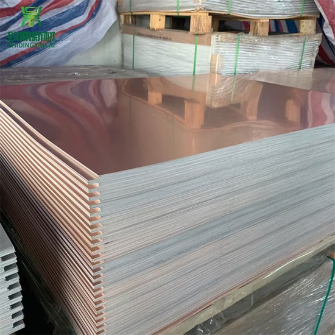
- Flex Substrate: Polyimide (PI) film (most common, high temp resistance up to 300°C+).
- Copper: Rolled Annealed (RA) copper preferred for flexibility over Electrodeposited (ED).
- Coverlay: Polyimide film with adhesive (instead of solder mask) for protection.
- Stiffeners: FR-4, stainless steel, or aluminum for component areas.
- Adhesive: Acrylic or epoxy (adhesiveless preferred for thinner, more reliable builds).
- Critical Design Considerations1. Bend Radius (Most Important Rule)Calculate minimum bend radius to prevent copper cracking:
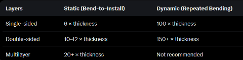
- Always keep the neutral bend axis (center of stack) in mind.
- Dynamic flex: Limit to 1–2 layers maximum.
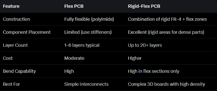
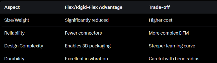
Flex vs. Rigid-Flex Comparison
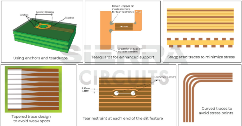
2. Trace Routing in Flex Areas
- Route traces perpendicular to the bend axis.
- Use curved traces instead of 90° corners.
- Stagger traces on different layers (avoid I-beaming/stacking).
- Add teardrops at pad-to-trace junctions.
- Use cross-hatched ground planes (instead of solid) to maintain flexibility.
3. Vias & Holes
- Avoid vias in bend zones (high risk of cracking).
- Keep plated through-holes (PTH) at least 20–50 mils (0.5–1.27 mm) away from bend areas.
- Use larger annular rings in flex.
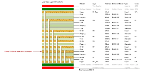
4. Rigid-Flex Stackup Best Practices
- Place flex layers in the center of the stackup (symmetrical construction).
- Use even layer counts to prevent warpage.
- Specify no-flow prepreg in rigid areas only.
- Design gradual transitions between rigid and flex zones.
- Maintain at least 0.5–1 mm clearance from rigid-flex boundary for components/traces.
5. Mechanical Features
- Add tear stops, fillets, or radius corners to prevent tearing.
- Use stiffeners under components on flex sections.
- Include alignment holes and fiducials.
- Define bend lines clearly in documentation.
6. Electrical & Thermal
- Impedance control possible but requires manufacturer-specific calculation (different dielectrics).
- Thermal management: Flex has lower conductivity — use thicker copper or heat sinks on rigid areas.
- EMI shielding: Add copper or silver ink layers if needed.
- Typical Design Rules (Manufacturer-Dependent)
- Minimum trace width/space: 3–5 mils (75–125 µm) in flex.
- Minimum bend radius: As per table above.
- Panel size limits: Flex materials have panel size constraints.
- Always request stackup and DFM review early from your fab.
- Manufacturing & Assembly Tips
- Flex circuits are more sensitive to handling — specify shipping in flat or rolled form.
- Higher reflow temperatures may be needed; use high-temp components.
- Test for bend cycles if dynamic application.
- Documentation: Clearly mark flex/rigid zones, bend lines, and stiffener locations in Gerber/ODB++ files.
Flex vs Standard Rigid Summary
Designing Flex or Rigid-Flex requires close collaboration with your manufacturer from day one. Tools like Altium Designer have excellent rigid-flex support with zone-based stackups and 3D folding previews.